- 您现在的位置:买卖IC网 > Sheet目录1992 > CYW305OXC (Silicon Laboratories Inc)IC CLOCK W305 SOLANO 56SSOP
W305B
........................ Document #: 38-07262 Rev. *B Page 3 of 20
Overview
The W305B is a highly integrated frequency timing generator,
supplying all the required clock sources for an Intel archi-
tecture platform using graphics integrated core logic.
Functional Description
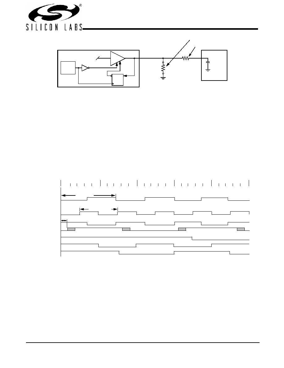
I/O Pin Operation
Upon power-up the power on strap option pins act as a logic
input. An external 10-k
strapping resistor should be used.
Figure 1 shows a suggested method for strapping resistor
connections.
After 2 ms, the pin becomes an output. Assuming the power
supply has stabilized by then, the specified output frequency
is delivered on the pins. If the power supply has not yet
reached full value, output frequency initially may be below
target but will increase to target once supply voltage has stabi-
lized. In either case, a short output clock cycle may be
produced from the CPU clock outputs when the outputs are
enabled.
Offsets Among Clock Signal Groups
relationship among the different groups of clock outputs from
W305B under different frequency modes.
Power-on
Reset
Timer
Output Three-state
Data
Latch
Hold
QD
W305B
Clock Load
Output
Buffer
10 k
Output
Low
Output Strapping Resistor
Series Termination Resistor
Figure 1. Input Logic Selection Through Resistor Load Option
Figure 2. Group Offset Waveforms (66-MHz CPU Clock, 100-MHz SDRAM Clock)
CPU 66-MHz
SDRAM 100-MHz
3V66 66-MHz
PCI 33-MHz
REF 14.318-MHz
USB 48-MHz
APIC 16.6-MHz
0 ns
CPU 66 Period
SDRAM 100 Period
Hub-PCI
40 ns
30 ns
20 ns
10 ns
发布紧急采购,3分钟左右您将得到回复。
相关PDF资料
DAC5674IPHPG4
IC DAC 14BIT 400MSPS 48-HTQFP
DAC7621EBG4
IC SNGL 12BIT PARALLEL D/A 20SSO
DAC7801KPG4
IC DUAL 12BIT CMOS DAC 24-DIP
DAC8043AESZ
IC DAC 12BIT MULT SRL INP 8SOIC
DAC8043GP
IC DAC 12BIT MULTIPLY CMOS 8-DIP
DAC8221GP
IC DAC 12BIT DUAL W/BUFF 24-DIP
DAC8222GPZ
IC DAC 12BIT DUAL W/BUFF 24DIP
DAC8229FSZ-REEL
IC DAC 8BIT DUAL V-OUT 20SOIC
相关代理商/技术参数
CYW305OXCT
功能描述:时钟发生器及支持产品 Legacy-Sys Clk Intel RSolano Chip W305B RoHS:否 制造商:Silicon Labs 类型:Clock Generators 最大输入频率:14.318 MHz 最大输出频率:166 MHz 输出端数量:16 占空比 - 最大:55 % 工作电源电压:3.3 V 工作电源电流:1 mA 最大工作温度:+ 85 C 安装风格:SMD/SMT 封装 / 箱体:QFN-56
CYW311OXC
功能描述:时钟发生器及支持产品 Sys Clk VIATM Pro266 DDR Chipset W311 DS RoHS:否 制造商:Silicon Labs 类型:Clock Generators 最大输入频率:14.318 MHz 最大输出频率:166 MHz 输出端数量:16 占空比 - 最大:55 % 工作电源电压:3.3 V 工作电源电流:1 mA 最大工作温度:+ 85 C 安装风格:SMD/SMT 封装 / 箱体:QFN-56
CYW311OXCT
功能描述:时钟发生器及支持产品 Sys Clk VIATM Pro266 DDR Chipset W311 DS RoHS:否 制造商:Silicon Labs 类型:Clock Generators 最大输入频率:14.318 MHz 最大输出频率:166 MHz 输出端数量:16 占空比 - 最大:55 % 工作电源电压:3.3 V 工作电源电流:1 mA 最大工作温度:+ 85 C 安装风格:SMD/SMT 封装 / 箱体:QFN-56
CYW312OXC
制造商:SPECTRALINEAR 制造商全称:SPECTRALINEAR 功能描述:FTG for VIA⑩ K7 Series Chipset with Programmable Output Frequency
CYW312OXCT
制造商:CYPRESS 制造商全称:Cypress Semiconductor 功能描述:FTG for VIA⑩ K7 Series Chipset with Programmable Output Frequency
CYW320OXC-3
功能描述:时钟合成器/抖动清除器 Legacy, W320-03 datasheet RoHS:否 制造商:Skyworks Solutions, Inc. 输出端数量: 输出电平: 最大输出频率: 输入电平: 最大输入频率:6.1 GHz 电源电压-最大:3.3 V 电源电压-最小:2.7 V 封装 / 箱体:TSSOP-28 封装:Reel
CYW320OXC-3T
功能描述:时钟合成器/抖动清除器 Legacy, W320-03 datasheet RoHS:否 制造商:Skyworks Solutions, Inc. 输出端数量: 输出电平: 最大输出频率: 输入电平: 最大输入频率:6.1 GHz 电源电压-最大:3.3 V 电源电压-最小:2.7 V 封装 / 箱体:TSSOP-28 封装:Reel
CYW320OXC-4
功能描述:时钟合成器/抖动清除器 Legacy, W320-04 datasheet RoHS:否 制造商:Skyworks Solutions, Inc. 输出端数量: 输出电平: 最大输出频率: 输入电平: 最大输入频率:6.1 GHz 电源电压-最大:3.3 V 电源电压-最小:2.7 V 封装 / 箱体:TSSOP-28 封装:Reel